PCB industry competition pattern is dispersed, China’s largest output value, the fastest-growing. Product category, the ordinary PCB profits thin as paper, profitability is not optimistic. Today, the layout of overseas PCB leading high-priority multi-layer PCB, flexible circuit board and the combination of soft and hard board, wide application areas, high value, market potential.
CCL is the most important raw material for PCB manufacturing, bargaining power is strong, and the high concentration of industry (the top five suppliers in the market share of about 50.1%), leading manufacturers bargaining power.
Mainland China has the highest proportion of CCL production in the world. However, its value-added products are low. High-end products depend on imports. The industrial structure is in the process of adjustment. Leading manufacturers are the first to achieve high value-added technology breakthroughs.
The upstream?copper prices into the cycle, brings?CCL and PCB enterprises new pricing opportunities.
Electrolytic copper foil is an important component of CCL and PCB. The electrolytic copper production capacity in the world and in Mainland China has not expanded in the past two years, but the capacity utilization rate has been increasing year by year.
Electrolytic copper foil has also been used as a lithium ion battery anode material collector, in recent years, the explosive growth of new energy vehicles, driven by lithium battery copper market in short supply, copper foil manufacturers have converted lithium foil, diversion part of the standard copper foil production capacity, Resulting in the supply of copper foil upstream PCB tension, sustained price increases, and has been transferred to the CCL and PCB link.
Copper prices, CCL and PCB manufacturers brings?new pricing opportunities, CCL leading enterprises and high-end PCB suppliers in the process of cost-shifting to expand profit margins, to obtain performance flexibility to improve. Copper foil prices have brought the history of copper clad laminate and PCB enterprises to enhance gross margins, related companies rose 3-5 times share price.
Industry needs to pick up, into a new round of the economic cycle. The number of sub-sectors of the PCB downstream market demand for double-digit annual growth rate, a PCB industry growth momentum.
The rapid development of the automotive PCB market, automotive PCB market scale of up to 100 billion, but the certification cycle is long, the threshold is high; new energy vehicles bring PCB demand billions incremental market; small spacing LED market rapid expansion, more Layer PCB board demand; mobile communication technology with each passing day, the construction of high-density small base stations to drive high value-added PCB needs; China’s high-end server market growth, increasing PCB value added.
]]>1, automatic soldering machine soldering temperature and suspend the use of precautions,?Automatic soldering machine in the welding temperature should be as low as 400 ℃, the middle of the machine should be closed when the welding machine and thermostat power supply and tin to the tip, to avoid the machine air burning, and iron head should always keep tin.
2, automatic soldering iron tip should always clean up;?If the tin part of the tip contains black oxide, can be coated with a new tin layer, and then clean the wet sponge clean tip. The cleaning is repeated until the oxide is completely removed and then a new tin layer is applied. And regularly clean the tip.
3, automatic soldering iron tip selection and welding: Automatic soldering machine in the welding, the soldering iron head can not be forced to pick or squeeze the welding objects, cleaning tip application of the original / professional manufacturer of clean sponge, and add some water, add water, squeeze dry, to keep the sponge wet Can be.
4, automatic soldering iron tip to keep the surface clean: Do not remove any excess solder from the tip of the soldering iron prior to shutting down the soldering station. This excess tin protects the surface of the tin from heat when the tip is hot, preventing oxidation. Do not add any compound to the surface.
5, automatic soldering iron tip to do other uses:?Because the relationship between the electroplating, the tip is absolutely not to use a knife file or grinding, not rub coarse iron head. It is recommended that fresh solder is applied to the tip of the soldering iron for the first time in order to remove the oxide on it.
6, automatic soldering machine should be promptly replaced tip,?With the automatic soldering machine with the longer, the tip will be small-scale deformation and re-erosion, this time must be replaced tip, otherwise there will be a large number of non-scale products
]]>Optimizing Return Paths
Techniques for Optimizing Return Paths
First of all, what is a return path? The ground plane is the simple answer. For every wave of energy (measured in volts) that goes out from a source, an equal but oppositely charged wave tries to make it back from the far end to the source. This counter-wave completes the circuit so that more waves of energy can follow. I say “tries” as the voltage seeks the path of least resistance.
Return on Layer Two?
That return path may or may not be the one that was designed for the circuit. A poorly designed return path will result in the return currents wandering around and escaping as electromagnetic interference. This phenomenon annoys other devices, messing with sound and picture quality among other things. The Federal Communications Commission has a threshold for these emissions. An acceptable product will be immune from the emissions of other products and will not disturb those products with its own emissions. Pretty simple to explain and often difficult to implement. Curbing EMI is one of the most important aspects of return path design.
In an alternating current (AC) application, the return path alternates from one of the two wires to the other. One wire has a positive voltage that swings negative while the other goes from a negative voltage to a positive voltage of the same value as the positive lead such as plus or minus 110 VAC. A three wire system, like you would see on power tools and HiFi gear, has that third lead at (or near) zero volts. That is considered “neutral” as it should not have any significant energy transfer going on. The third “rail” is there specifically to tie the chassis to the ground so that you, the user, do not become the ground path through an internal short within the equipment. Any time you are being used as a conductor, you’re probably having a bad day.
Cause and effect are in play with direct current (DC) as well. What’s missing is the reciprocal action that promotes energy transfer over great distances. What’s left is a cleaner medium to work in. Without AC noise, we can turn our power on and off in an established pattern to do useful things. Morse code is still relevant as a machine language, but the data rate makes the return path of little concern. ASCII and other binary code zip around in massive bursts on our devices and beyond. The switching speeds are somewhere between ridiculous and ludicrous. It is in this world that completing the whole circuit really matters.
The Thin of the Plot
Our best defense against the losses through emissions is to make the current loops as short as possible. Bias circuits require bypass caps to complete the loop. It is not enough to place the capacitor near the power pin and call it a day. The orientation of the cap should be considered if there is a ground pin in the vicinity. A low-impedance trace to that pin or to a common ground via will be a good move.
Even if the layout at hand is low tech and can get away with a quick and dirty execution, it still has to share a world where other devices do their thing without interruption.
Better still for power supplies is to bridge the power pin to the ground pad under the regulator with the capacitor acting as a direct part of the path. I know that the assembly house will advise you to place all of the components in the same orientation. It is so rare for that method to lead to the optimal performance, that I’ve done a placement that way approximately zero times out of thousands of PCB Designs. The end user’s right to the best possible performance comes before the factory’s guidelines; at least to a point. This holds true especially for analog, but digital designs quite often have edge rates that require optimal placement just to get over the threshold of minimum performance.
Even if the layout at hand is low tech and can get away with a quick and dirty execution, it still has to share a world where other devices do their thing without interruption. One of the other things that I don’t buy into is the notion that something doesn’t need much care because it’s just a prototype or a test fixture. Bologna! Science projects have almost as much chance at becoming a product as the projects that were intended for eventual production. Always be prepared for a design to “go viral” and for the stakeholders to be reluctant to have you make any further changes. It has happened before and will happen again.
Routing Whoahs!
Before you route over a gap in the plane, have a look at some of the simulation videos available online. A broken Faraday cage generates an alarming field of electromagnetic interference or EMI. The bad design work itself does not make the radiation. The power source of the equipment drives the radiation and is enabled by the leaky design.. That’s right, you pay extra in power inefficiency in order to fail FCC certification. Fix the mess before it becomes one.
A light bulb doesn’t emit any photons until you flip the switch. The switching regulator is not so different. Installing it near the device that loads the regulator’s output pin will help minimize the obnoxious current flow around the area. Yes, it is noisy by nature, but it can be contained. All of the good vendors show you how to be successful using their product. They are going to be conservative and use more space that you might be able to allocate. Good (ground) fences make good neighbors in this case.
Optimal return paths help devices coexist. A little bit of space won or lost can make a lot of difference. The formula for coupling is a nonlinear function such that doubling the air-gap between two items results in a square of the isolation. Likewise, sliding two traces just a little closer to each other can dramatically increase the amount of cross-talk on those lines. This, by itself, is reason enough for those stakeholders to get squeamish when you want to “DFM” their “science project”. Risk aversion rises as we go along the product life cycle so it pays to be brave and do it right as soon as you can. From placement to fan-out through routing and tape-out, design each connection as a whole circuit. It is always more gratifying to tell a success story. Make it happen.
]]>
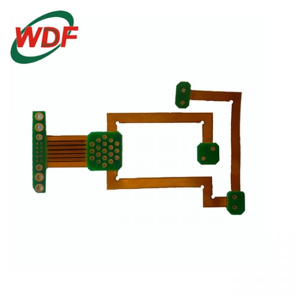
Rigid-flex circuits combine standard circuit board construction with flexible design for situations that require more durability. Have you ever wondered about the materials and layouts involved in the creation of these versatile PCBs? This blog post will provide a quick overview of common materials and constructions in flex and rigid-flex PCBs.
Materials Used in Flex Circuits
While most standard PCBs have a fiberglass or metal base, flex circuit cores consist of a flexible polymer. The majority of flex PCBs have a polyimide (PI) film as a substrate. PI film does not soften when heated, but it stays flexible after thermosetting. Many thermosetting resins like PI become rigid after heating, making PI a superior material in flex PCB construction. Standard PI film does not have good resistance to humidity and tears, but choosing upgraded PI film mitigates these issues.
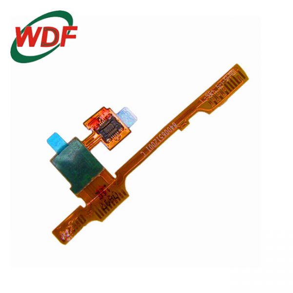
A flex PCB also requires an adhesive or special base material for its layers to attach. Manufacturers previously used adhesives only, but this method reduced the PCB’s reliability. To resolve these issues, they developed adhesiveless PI that attaches to copper without an adhesive. This material allows for thinner designs with a lower risk of via breakage. Instead of using a solder mask to cover and protect a flex circuit, manufacturers use a coverlay film also created with PI. If you want the area on the flex pcb to be rigid, the manufacture can laminate a stiffer to that portion, but the signal cannot travel between the flex and the stiffer.
Rigid-Flex PCB Materials
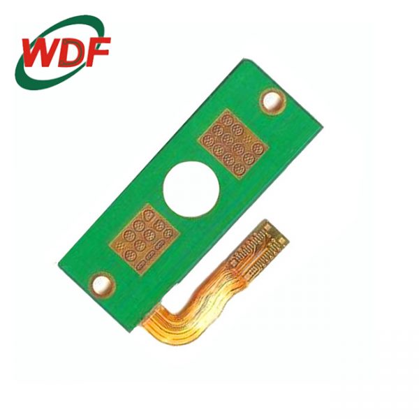
A rigid-flex PCB connects rigid PCB materials to flex materials. The result bends only in certain places, making the board stronger yet still flexible. If you want the signal to transfer between the rigid and flex part you will need to design a rigid flex pcb. In a rigid-flex design, the flexible part of the board resembles a typical flex circuit. Meanwhile, the rigid sections have similar materials to standard rigid PCBs. Just like standard PCBs, these rigid areas often have fiberglass as a substrate material. Multilayer rigid-flex PCBs also include prereg fiberglass as middle substrate layers.
Popular Stackups for Layer Flex Circuit Construction
Single- and double-layer flex circuits each have common stackups found in many electronics. A single-layer flex circuit often includes stiffeners created from pressure-sensitive adhesive (PSA) and FR-4 fiberglass. Pieces of FR-4 stabilize each end of the PCB, while a thin layer of PSA adds sturdiness to the middle of the board. Since double-layer flex PCBs have multiple computer-related applications, they tend to have zero insertion force (ZIF) connectors. Using PI as stiffeners at the ends gives the board the flexibility needed to attach to the ZIF connector.
Rigid-flex PCBs have various constructions, but one common approach involves four rigid layers and two flexible ones. It includes a core made from adhesiveless PI that reduces breakage risks. Above this layer and its copper film, two layers of prepreg connect to the flex section’s coverlay adhesive and coverlay layers. The rigid sections receive additional layers of copper, fiberglass and solder mask.
]]>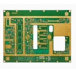
- Brand Name: Customized
- Min.Order Quantity:?No
- Supply Ability:?30~50 thousand ㎡/Month
- Port:?Shenzhen
- Service:?EMS/OEM/ODM
- Payment Terms:?T/T,Paypal,WU etc.
- Layer:?2
- Base Material:?FR4
- Copper Thickness:?1oz
- Board Thickness:?1.6mm
- Solder Mask Color:?Green(can customized)
- Silkscreen Color:?White(can customized)
- Surface Finishing:?HASL-LF
- Test Way:?100% E-Test
PRODUCT DETAIL
——————————————————————————————————————————————————————–
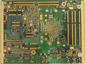
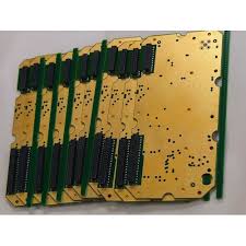
Short Description:
- Brand Name: Customized
- Min.Order Quantity:?No
- Supply Ability:?30~50 thousand ㎡/Month
- Port:?Shenzhen
- Service:?EMS/OEM/ODM
- Payment Terms:?T/T,Paypal,WU etc.
- Layer:?16
- Base Material:?High Tg FR4
- Copper Thickness:?1oz
- Board Thickness:?2.43mm
- Solder Mask Color:?Green(can customized)
- Silkscreen Color:?White(can customized)
- Surface Finishing:?Immersion Gold
- Application Industry:?Industrial Control
- Application Products:?Core board
- Outer Line width/space:?4/4mil
- Inner Line width/space:?3.5/3.5mil
- Min.Hole Size:?0.75mm
- Test Way:?100% E-Test
- Standard:?IPC-Class2/Class 3
PRODUCT DETAIL
——————————————————————————————————————————————————————–