- Brand Name: Customized
- Min.Order Quantity:?No
- Supply Ability:?30~50 thousand ㎡/Month
- Port:?Shenzhen
- Service:?EMS/OEM/ODM
- Payment Terms:?T/T,Paypal,WU etc.
- Layer:?16
- Base Material:?High Tg FR4
- Copper Thickness:?1oz
- Board Thickness:?2.43mm
- Solder Mask Color:?Green(can customized)
- Silkscreen Color:?White(can customized)
- Surface Finishing:?Immersion Gold
- Application Industry:?Industrial Control
- Application Products:?Core board
- Outer Line width/space:?4/4mil
- Inner Line width/space:?3.5/3.5mil
- Min.Hole Size:?0.75mm
- Test Way:?100% E-Test
- Standard:?IPC-Class2/Class 3
PRODUCT DETAIL
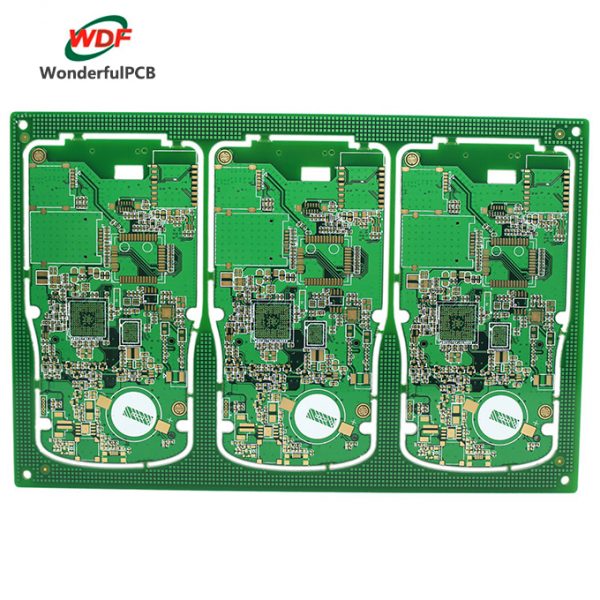
6 layers boards fr4 94v0 rohs pcb for the fingerprint Scanner
Advantages
–?No MOQ
– OEM services provided
–?Heavy copper PCB,?Heavy gold PCB,?Blind / Buried via PCB,?High layer count PCB? manufacturable
– Factory direct price
– Replying with price?in?one working day
– Shipping?within 24 hours
– Certificate: ROHS, UL, ISO9001-2000, ISO14001,SGS Lead-Free
PCB Capacity
| PCB General Capability | |
| Number of Layer | 1 – 20 Layer |
| Maximum Processing Area | 680 × 1000MM |
| Min Board Thickness | 2 Layer – 0.3MM ( 12 mil ) |
| 4 Layer – 0.4MM ( 16 mil ) | |
| 6 Layer – 0.8MM ( 32 mil ) | |
| 8 Layer – 1.0MM ( 40 mil) | |
| 10 Layer – 1.1MM ( 44 mil ) | |
| 12 Layer – 1.3MM ( 52 mil ) | |
| 14 Layer – 1.5MM ( 59 mil ) | |
| 16 Layer – 1.6MM ( 63 mil ) | |
| 18 Layer – 1.8MM ( 71 mil ) | |
| Finished Board Thickness Tolerance | Thickness ≤ 1.0MM, Tolerance: ± 0.1MM |
| 1.0MM ≤ Thickness ≤ 6.5MM, Tolerance ± 10% | |
| Twisting and Bending | ≤ 0.75%, Min: 0.5% |
| Range of TG | 130 – 215 ℃ |
| Impedance Tolerance | ± 10%, Min: ± 5% |
| Hi-Pot Test | Max: 4000V/10MA/60S |
| Surface Treatment | HASL, With Lead, HASL Free Lead |
| Flash Gold, Immersion Gold | |
| Immersion Silver, Immersion Tin | |
| Gold Finger, OSP | |
| PCB Cu Thickness + Plating | |
| Out Layer Cu Thickness | 1 – 6OZ |
| Inner Layer Cu Thickness | 0.5 – 4OZ |
| Cu Thickness of PTH | 20UM ≤ Average ≤ 25UM |
| Min: 18UM | |
| HASL with Lead | Tin 63% Lead 37% |
| HASL Free Lead | 7UM ≤ Surface Thickness ≤ 12UM |
| Thick Gold Plating | Ni Thickness: 3 – 5UM ( 120u” – 200u” ) |
| Gold Thickness: 0.025 – 1.27UM ( 1u” – 50u” ) | |
| Immersion Gold | Ni Thckness: 3 – 5UM ( 120u” – 200u” ) |
| Gold Thickness: 0.025 – 0.15UM ( 1u” – 3u” ) | |
| Immersion Silver | Ag Thickness: 0.15- 0.75 UM ( 6u” – 30u” ) |
| Gold Finger | Ni Thickness: 3 – 5UM ( 120u” – 160u” ) |
| Gold Thickness: 0.025 – 1.51UM ( 1u” – 60u” ) | |
| U940 PCB Pattern Limit Capability | |
| Min Width | 0.075MM ( 3 mil ) |
| Min Trace | 0.075MM ( 3 mil ) |
| Min Width of Ring ( Inner Layer ) | 0.15MM ( 6 mil ) |
| Min Width of Ring ( Out Layer ) | 0.1MM ( 4 mil ) |
| Min Solder Bridge | 0.1MM ( 4 mil ) |
| Min Height of Legend | 0.7MM ( 28 mil ) |
| Min Width of Legend | 0.15MM ( 6 mil ) |
| PCB Holes Processing Capability | |
| Final Hole Size | Min: Laser 0.1MM, Machine 0.2MM |
| Drilling Hole Size | 0.10 – 6.5MM |
| Drilling Tolerance | NPTH: ±0.05MM, PTH: ±0.075MM |
| Final Hole Size Tolerance ( PTH ) | φ0.20 – 1.60MM ± 0.075MM |
| φ1.60 – 6.30MM ± 0.10MM | |
| Final Hole Size Tolerance ( NPTH ) | φ0.20 – 1.60MM ± 0.05MM |
| φ1.60 – 6.50MM ± 0.05MM | |
| Drilling Strip Hole | -0L ~tu.’gth /width 2:1 |
| Min Strip Hole Width 0.65MM | |
| Length & Width Tolerance ± 0.05MM | |
| Board Thickness / Hole Size | ≤ 10:1 |
| PCB Cover Thickness Capability | |
| Solder Mask Color | Green,Matte Green,Yellow,Blue,Red,Black,Matte Black,White |
| Solder Mask Thickness | Surface Line ≥ 10UM |
| Surface Line Corner ≥ 6UM | |
| Surface Board 10 – 25UM | |
| Solder Mask Bridge Width | |
| Legend Color | White,Yellow,Black |
| Min Height of Legend | 0.70MM ( 28 mil ) |
| Min Width of Legend | 0.15MM ( 6 mil ) |
| Blue Gel Thickness | 0.2 – 1.5MM |
| Blue Gel Tolerance | ±0.15MM |
| Carbon Print Thickness | 5 – 25UM |
| Carbon Print Min Space | 0.25MM |
| Carbon Print Impedance | 200Ω |
| Blind/Burried/Half Via PCB Capability | |
| Parameters | (1+1)e.g.(4-layer)blind via:1-2,2-4
(6-layer)buried via:2-3,3-4 (8-layer)blind/buried:1-3,4-5,6-8 |
| Min Via | Laser 0.1MM, Machine 0.2MM |
| Half Via | Min: 0.6MM |
| Impedance Capability | |
| Resistance Value | Single-ended 50 – 75Ω, Difference 100Ω, Coplanar 50 – 75Ω |

